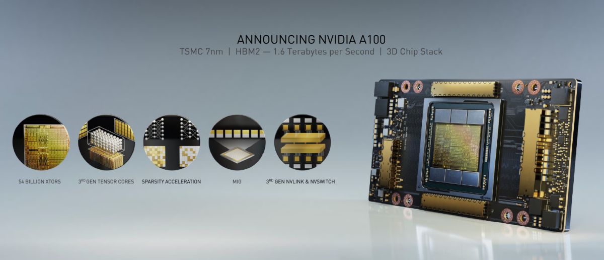
Getting right into it, the A100’s Ampere GPU is based on a 7nm die lithography, courtesy of TSMC. Additionally, GPU contains a whooping 54 billion transistors, all within a die area of 826mm2. For memory, NVIDIA has given it a total of 40GB of HBM2. Like its predecessor, the card has access to NVIDIA’s NVLink technology, allowing it to be paired with multiple A100 modules while maintaining speeds of up to 600GB/s.
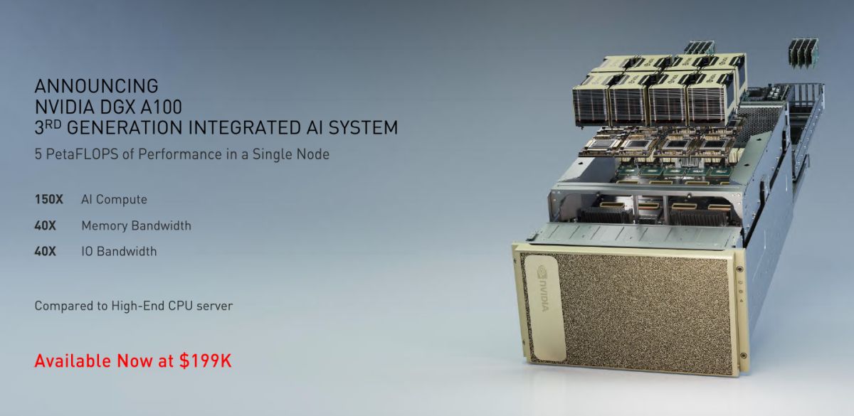
In regards to its performance, NVIDIA says that the A100 is capable of achieving up to 312 TFLOPS in FP32 training, 19.5 TFLOPS in FP64 HPC, and 1248 TOPS in INT8 Inference operations. By comparison, NVIDIA says that Ampere is approximately 20 times more powerful and more efficient than its last generation supercomputer GPU, Volta. In conjunction with the A100, NVIDIA also announced the DGX A100, its 3rd generation supercomputing GPU solution. Like the DGX-2, the DGX A100 is a beast, comprising a total of eight A100 GPUs, a 15TB Gen4 NVMe SSD and more importantly, it comes with nine Mellanox ConnectX-6 LAN Network Interface. The latter being a technology stemming from NVIDIA’s acquisition of Mellanox Technologies last year.
Of course, the DGX A100 is clearly aimed towards institutions in the field of science; places that require a massive amount of raw computing power. Enough to make the most complex and daunting of calculations and problems. That said, if you’re looking at building your first datacentre with this machine, be prepared to fork out a whopping US$199000 (~RM863759) for one unit. On a related note, you can catch the GTC 2020 keynote via NVIDIA’s official YouTube channel. It’s broken down into eight videos, and features its CEO, Jen-Hsun Huang, doing the presentation. (Source: NVIDIA)

